Buck 2 click – MikroElektronika Step Down DC-DC Switching Regulator MikroElektronika
$ 30,00 $ 18,00
Buck 2 click – MikroElektronika Step Down DC-DC Switching Regulator
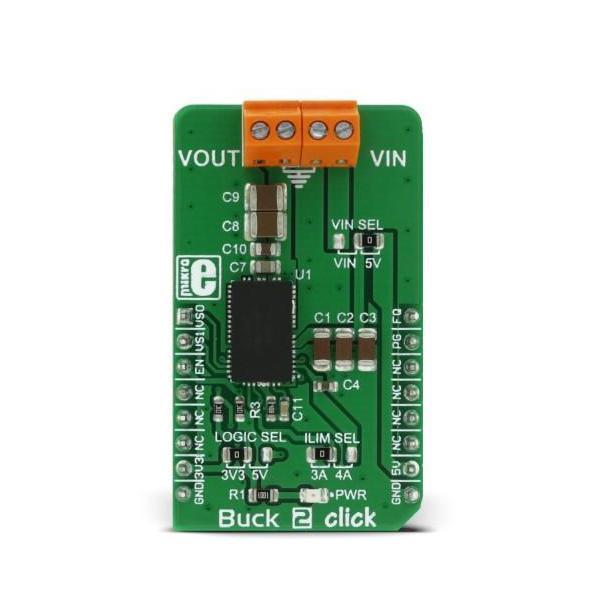
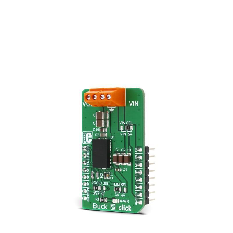
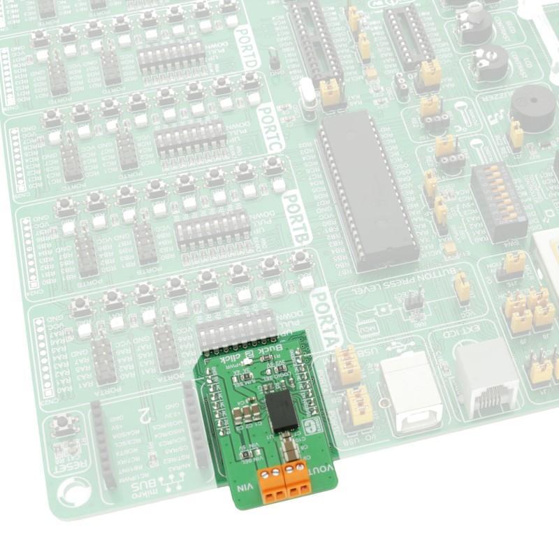
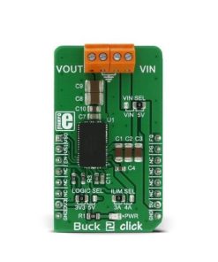
Buck 2 click is a powerful step down DC-DC switching regulator. It gives a high precision regulated voltage at its output and it can handle an ample amount of current. Buck 2 click is highly configurable – the output voltage, maximum current limiting, and the switching frequency parameters can be controlled via the IC pins routed to the mikroBUS™ socket, providing a simple and secure connection to the host MCU.
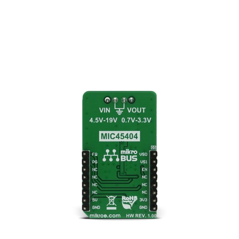
The input voltage can range from 4.5V to 19V and the output can be set to work in several discrete steps, ranging from 0.7V to 3.3V. Features, such as the wide range of input voltages, pin configurable working parameters, internal soft start, thermal shutdown, hiccup mode short-circuit protection and high switching efficiency, make this device a perfect choice for any step-down application which demands reasonably high current and accurate voltage regulation with clean and ripple-free low voltage power supply – such as the embedded electronic devices, servers, routers, data storage devices, low power ICs and similar.
How does it work?
The step down DC-DC regulator used on this click board™ is the MIC45404, a 19V 5A ultra-low profile DC-to-DC power module by Microchip. This IC is a valley current mode controlled power module, meaning that it has a faster response than the traditional peak current mode control, thus better response to transients. This IC requires a minimal number of external components, which makes the whole device pretty robust and easy to work with. Unlike other traditional switching regulators, this one does not require external feedback components – it is enough to directly connect the OUTSNS pin to the output voltage. This allows for more accurate control over the voltage regulation.
Buck 2 click offers a possibility to configure certain working parameters such as the output voltage, current limit threshold, and PWM switching frequency, by changing the states of the dedicated pins. Those pins are either routed to the mikroBUS™ socket or equipped with the SMD jumpers so that they could be set by the end user. These pins can be set to the GND level, VCC level or can be left afloat – high impedance mode (HIGH-Z). They are sampled as soon as the internal voltage is stabilized, and their state is latched – further changes will not affect the selected configuration. Tables for the configurable pins settings and their values can be found below.
Output voltage level is selected by the VOSET0 and VOSET1 pins of the MIC45404 IC, routed to the mikroBUS™ AN and RST pins, respectively. This gives a total of nine possible voltage level combinations.

PWM switching frequency can be changed by the FREQ pin, routed to the PWM pin of the mikroBUS™ socket. The switching frequency is related to the selected output voltage and for this reason, it is routed to the mikroBUS™ socket, so that the voltage output and the corresponding frequency for the selected voltage can be set. There are three possible frequency values: 400kHz, 565kHz, and 790kHz.
The current limiting is selected by the onboard SMD jumper, labelled as ILIM SEL. It is possible to limit the current to 3A, 4A, and 5A. The current limiting is instantaneous and the MIC45404 IC offers current limit and current sensing on both high-side and low-side internal MOSFET switches. It also features a special Hiccup mode, which reduces power dissipation in prolonged overload or short circuit situations. When a low-end MOSFET current limiting event occurs, the internal counter is incremented. A PWM cycle with no low-end MOSFET limiting events will decrease the internal counter. If the internal counter reaches 0Fh, both MOSFETs will be tri-stated and the power to the output will be cut off. After a predetermined wait time has expired, the MIC45404 IC will be restarted and will attempt a new soft-startup sequence. This mechanism ensures that no false overload events are generated.
The EN/DLY pin is used to enable the device. A HIGH logic level on this pin will start up the internal sections of the MIC45404 IC. This pin is routed to the mikroBUS™ CS pin, and since it is in an open drain configuration, it is pulled by the resistor to the GND.
The PG pin is used to indicate the power good condition of the output. When the voltage on the output (OUTSNS) drops under 90% of the regulated voltage, this pin is set to a LOW logic level, indicating irregular output voltage. This pin is pulled to a HIGH logic level by an on-board pull-up resistor since it is configured as the open drain output. It is routed to the mikroBUS™ INT pin.
Buck 2 click is equipped with two screw terminals, used to connect the input voltage source as well as the output load. The input voltage source is selectable between the +5V rail from the mikroBUS™ and the voltage at the input terminal. It also has an onboard LOGIC SEL SMD jumper, used to set up the logic voltage level, so that both 3.3V and 5V capable MCUs can be used.
Output voltage selection
| VOSET1 | VOSET0 | Output Voltage [V] | Required Sw. Freq. [kHz] |
|---|---|---|---|
| 0 | 0 | 3.3 | 790 |
| 0 | 1 | 2.5 | |
| 1 | 0 | 1.8 | 565 |
| 1 | 1 | 1.5 | |
| 0 | High-Z | 1.2 | 400 |
| High-Z | 0 | 1.0 | |
| 1 | High-Z | 0.9 | |
| High-Z | 1 | 0.8 | |
| High-Z | High-Z | 0.7 |
Switching frequency
| FQ pin | Frequency [KHz] |
|---|---|
| High-Z (open) | 400 |
| 0 (GND) | 565 |
| 1 (VDDA) | 790 |
Specifications
| Type | Buck |
| Applications | A perfect choice for step-down applications for embedded electronic devices, servers, routers, data storage devices, low power ICs, etc |
| On-board modules | MIC45404, a 19V 5A ultra-low profile DC-to-DC power module by Microchip |
| Key Features | Buck 2 click features a wide range of input voltages, pin configurable working parameters, internal soft start, thermal shutdown, hiccup mode short-circuit protection and high switching efficiency |
| Interface | GPIO |
| Input Voltage | 3.3V or 5V |
| Click board size | M (42.9 x 25.4 mm) |
Downloads
Fast Shipping and Professional Packing
Through our long-term relationship in a long-standing partnership with UPS, FedEx, DHL and many other top global carriers we can provide a variety of shipping options. Our warehouse employees will pack every item to our exacting specifications. The goods you send us are checked thoroughly and secured properly prior to shipping. Everyday we deliver thousands of packages to customers across many countries. The fact that we're committed to becoming the biggest online retailer in the world is clear. Both Europe as well as the USA have warehouses and distribution centres.
Orders that contain more than one item are assigned processing times in accordance with the item.
We will inspect each and every one of the items ordered before shipping. Today, most orders will be shipped within 48 hours. The delivery time should be between 3-7 days.
Returns
The stock market is always changing. It's not entirely managed by us, since we have multiple organizations, such as the factory and our storage. Stock levels can fluctuate at any given time. Please understand it may happen that your order will be out of stock after the order is placed.
The policy is for 30 days. If you have passed 30 days in the past since you purchased, unfortunately we can't offer you a refund or exchange.
To be eligible for a refund, your item must be in good condition and in the same state that you received it. The item must be in the original packaging.
Related products
Power Module
Power Module
Power Adaptor
Power Module
MIC23099 click – MikroElektronika Single AA/AAA Battery Cell Regulator MikroElektronika
Power Adaptor
Power Module
Serial Comms
Battery Holder
Power Module
Power Module
Power Module
Battery Holder
Battery Holder
Power Adaptor
Power Module
Battery Holder
Battery Holder
Battery Holder
Power Module
Solar Power Manager Embedded 10000mAh Li-Po Battery, Supports 6V~24V Solar Panels Waveshare
