MCP16331 INV click – MikroElektronika Buck-Boost Voltage Regulator MikroElektronika
$ 25,00 $ 15,00
MCP16331 INV click – MikroElektronika Buck-Boost Voltage Regulator
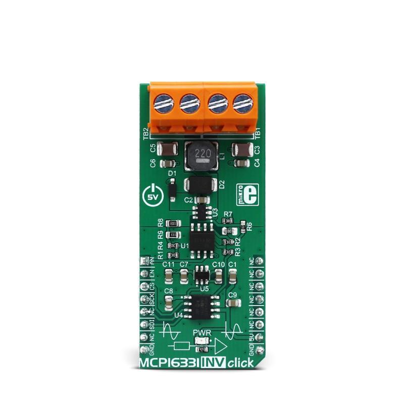
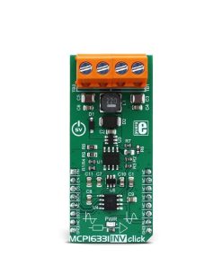
MCP16331 INV click works as a buck-boost voltage regulator, a switching regulator topology that combines principles of the buck conversion (step-down) and the boost conversion (step-up). A buck converter outputs voltage that is smaller than the input voltage (steps down the input voltage). A boost converter outputs voltage that is greater than the input voltage (steps up the input voltage). By combining these two topologies, MCP16331 INV click is able to output a regulated DC voltage, which can be set in the code, for input voltage both greater and less than the output voltage.
A major difference between the MCP16331 INV click and another click with the same name – MCP16331 click, is that this click works in an inverting configuration, providing an output voltage which is negative in respect to the GND level. Negative voltage is often used in symmetrical power supply configurations – for powering up operational amplifiers and similar devices that require such type of power supply. This feature, as well as the excellent power switching efficiency, overtemperature protection, and a clean regulated voltage output makes this device an ideal solution for powering up any application that demands a negative voltage power supply.
How does it work?
The switching regulator used on MCP16331 INV click is the MCP16331, a step-down (buck) switching regulator from Microchip. However, with the help of a few external components, MCP16331 INV click is able to regulate voltage levels both lower and higher than the input voltage, working as an inverted boost-buck voltage regulator.
The MCP16331 INV click is designed so that it can output a negative voltage, with respect to the GND. A negative voltage is often used in the analog electronics domain, to power up devices which require both positive and negative voltages to be applied. A good example would be an operational amplifier (opamp) which amplifies an AC signal. The signal goes in both positive and negative direction with respect to the GND. Processing this kind of signal with using just a single voltage source is difficult and requires workarounds such as using capacitors, charge pumps and virtual GNDs. Using a symmetrical power supply reduces the number of required components and simplifies the design.
To be able to deliver a negative voltage, several additional components, such as the ADM8828 voltage inverter IC and the LM318, a dual operational amplifier have to be added. The ADM8828 voltage inverter IC is used to provide a negative component of the symmetrical power supply, used for the LM318 dual opamp. One integrated opamp from the LM318 IC is used to invert the output from the DAC. The other opamp from the LM318 IC is used to invert the output from the voltage divider, located on the output rail of the MCP16331 so that it can be used by the MCU, which uses a single voltage power source.
To set the output voltage of the MCP16331 INV click, the MCP4921 – a low power 12-Bit dual voltage output DAC is used in the feedback loop. As already mentioned, it is necessary to invert this signal as the MCP4921 is supplied from a single voltage power supply, and it is not capable of bringing the signal lower than the GND. Since MCP16331 works in the negative voltage domain, the feedback voltage applied to the FB pin of this IC also needs to be negative with respect to the GND. One of the LM318’s integrated opamps, configured as a unity gain inverter, is used to invert the DAC output voltage.
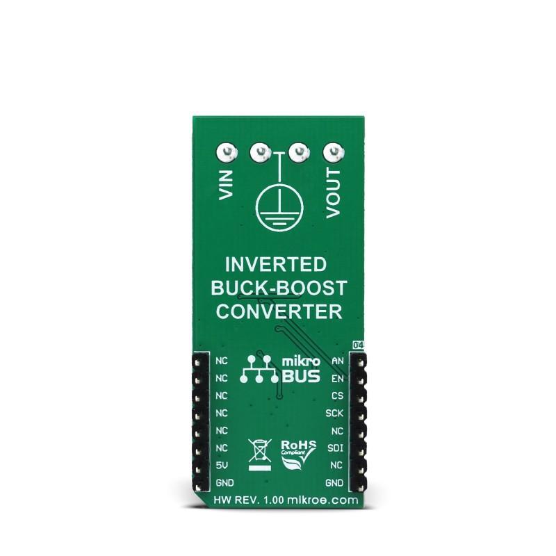
Since the FB pin of the MCP16331 IC is driven by the DAC, it is enough to set the DAC to a specific value, in order to control the output voltage of the click board™. Communication with the MCP4921 DAC is done via the SPI interface. SPI bus pins of the MCP4921 are routed to the mikroBUS™ for an easy and secure connection with the host MCU.
The AN pin of the mikroBUS™ is routed to a middle point of a voltage divider at the output. This voltage divider is used to scale down the output voltage so it can be successfully converted by the ADC of the host MCU. The voltage on the divider also has to be inverted, since it is coming out from the negative voltage domain. This is achieved by the second operational amplifier of the LM318 IC, which also works as a unity gain inverter. This value can be used to monitor the output voltage and correct it, if needed.
The EN pin of the MCP16331 switching regulator is routed to the mikroBUS™ RST pin. By pulling this pin to a HIGH logic level, the internal sections of the regulator are enabled. The EN pin is internally pulled to a HIGH logic level, so the device will be enabled, even if this pin is left floating. Therefore, a correct startup sequence must be used, in order to avoid undesirable effects (in the NOTE, below).
Although it is designed to work as the negative power supply, MCP16331INV click can also be used to drive a regular load, connecting its positive input terminal to the GND of the click board™, and using the negative output of the MCP16331INV click as the GND.
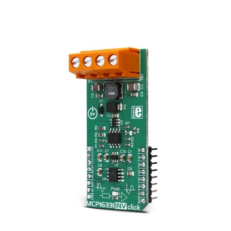
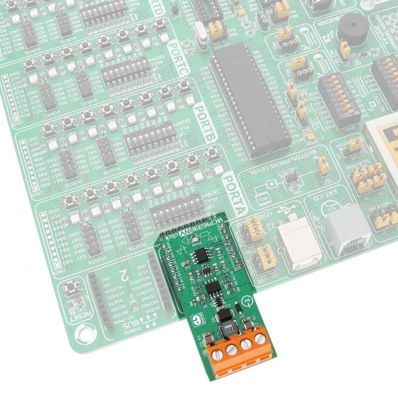
MCP16331 INV click comes with two screw terminals, used to connect the input and the output voltage rails. This click board™ uses only +5V rail from the mikroBUS™. Provided libraries demonstrate functionality of the MCP16331 INV click and offer an easy and simple way of setting it up. The included example can be used as a reference for future designs
NOTE: To avoid any possible damage to any load connected to the VOUT terminals, the correct power-up sequence must be followed:
- Disable the MCP16331 by setting the mikroBUS™ pin RST (EN) to a LOW logic level (GND)
- Set the desired output voltage via SPI (see the software section below)
- Enable the MCP16331 by setting the mikroBUS™ pin RST (EN) to a HIGH logic level (VCC)
The reason for this sequence is that the enable pin (EN) of the MCP16331 has an internal pull-up resistor which keeps the MCP16331 output stage enabled at all times, even if the pin is left unconnected. Having an undetermined voltage output at the DAC during the startup sequence might result with unwanted voltage levels at the output terminal.
Libraries, provided with the MCP16331 INV click, will allow for simple and effortless setup of the necessary parameters. The included demo application can be used as a reference for future designs, and it demonstrates the functionality of the click board™, as well as the included software libraries.
Specifications
| Type | Boost,Buck |
| Applications | Negative voltage is often used in symmetrical power supply configuration for powering up operational amplifiers and similar devices that require such type of power supply. |
| On-board modules | MCP16331, a step-down (buck) switching regulator, LM318, a dual operational amplifier, ADM8828, a switched-capacitor voltage inverter, MCP4921, a low power 12-Bit dual voltage output DAC |
| Key Features | Negative power supply source with very high switching efficiency, overvoltage protection, internal soft start, adjustable voltage, it can sustain a reasonably high current |
| Interface | GPIO,SPI |
| Input Voltage | 5V |
| Click board size | L (57.15 x 25.4 mm) |
Downloads
Fast Shipping and Professional Packing
Through our long-term relationship in a long-standing partnership with UPS, FedEx, DHL and many other top global carriers we can provide a variety of shipping options. Our warehouse employees will pack every item to our exacting specifications. The goods you send us are checked thoroughly and secured properly prior to shipping. Everyday we deliver thousands of packages to customers across many countries. The fact that we're committed to becoming the biggest online retailer in the world is clear. Both Europe as well as the USA have warehouses and distribution centres.
Orders that contain more than one item are assigned processing times in accordance with the item.
We will inspect each and every one of the items ordered before shipping. Today, most orders will be shipped within 48 hours. The delivery time should be between 3-7 days.
Returns
The stock market is always changing. It's not entirely managed by us, since we have multiple organizations, such as the factory and our storage. Stock levels can fluctuate at any given time. Please understand it may happen that your order will be out of stock after the order is placed.
The policy is for 30 days. If you have passed 30 days in the past since you purchased, unfortunately we can't offer you a refund or exchange.
To be eligible for a refund, your item must be in good condition and in the same state that you received it. The item must be in the original packaging.
Related products
Power Adaptor
Power Module
Power Module
Power Module
Solar Power Manager Embedded 10000mAh Li-Po Battery, Supports 6V~24V Solar Panels Waveshare
Battery Holder
Serial Comms
Battery Holder
Battery Holder
Battery Holder
Power Module
Power Module
Power Adaptor
Battery Holder
Power Module
Power Module
Power Module
MIC23099 click – MikroElektronika Single AA/AAA Battery Cell Regulator MikroElektronika
Power Adaptor
Power Module
Battery Holder
