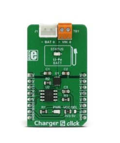
MIC33153 click – MikroElektronika DC-DC Adjustable Converter MikroElektronika
$ 25,00 $ 15,00
MIC33153 click – MikroElektronika DC-DC Adjustable Converter
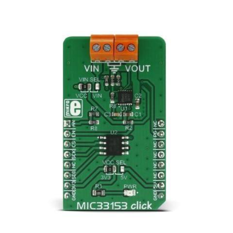
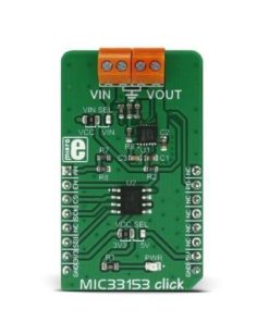
MIC33153 click is a DC-DC adjustable step-down (buck) converter that is designed to deliver a substantial amount of current to very demanding loads, with the voltage output up to 3.5V. The ultra-fast transient response and the ripple free output voltage are some of the main features of this DC-DC step-down converter. The proprietary HyperLight Load™ technology allows very efficient step-down conversion even for very light loads.
This adjustable DC-DC step-down converter click board™ has a very specific field of applications in which it gives the best results. Due to its ripple free voltage output and very high conversion efficiency, it is designed to be used as the power supply for the various portable GPS devices, mobile handsets, portable media and mp3 players, wireless LAN cards and similar applications that demand very clean power supply and high step down DC-DC conversion efficiency factor.
How does it work?
This click uses the MIC33153, a 4MHz DC-DC buck regulator with integrated inductor and Hyperlight Load™ technology, from Microchip. This integrated buck regulator requires a minimal number of external components, including the inductor. This simplifies the design greatly, retaining the advertised electrical characteristics. Also, thermal shutdown and current limit protection features ensure the safe operation, even in case of errors and short circuits.
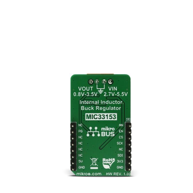
The click operates with the input voltage range from 2.7V up to 5.5V and it is capable to deliver a regulated output ranging from 0.8V to 3.5V, with up to 1.2A. The output voltage is selectable and it is managed by the voltage on the FB pin. This pin is routed to the output of the MCP4921, a 12bit DAC converter from Microchip, with the SPI interface. The voltage on the DAC output affects the FB pin voltage, which in return affects the main output voltage.
A voltage divider connected between the main output terminal and the GND, allows monitoring the output voltage via the AN pin of the mikroBUS™. This gives an insight of the output voltage condition: if the output voltage deviates from the desired value, the corrected value can be sent to the DAC. MCP4921 DAC converter has its SPI lines routed to the mikroBUS™ so it is enough to just send a new value via the SPI of the click board™ if a correction is needed. Of course, being a buck converter, the click board™ expects higher input voltage than it is set at its output.
The proprietary HyperLight Load™ technology allows to still operate with enough efficiency, when a very light load is connected to the output terminal. Instead of using the continuous PWM signal to operate the DC-DC buck converter, it goes into the discontinuous mode, with the pulse frequency modulation (PFM) signal used for regulating of the output. As the output current rises, the device enters the continuous conducting mode (CCM) with the PWM frequency at 4MHz. The transition is transparent and it happens automatically when the output current rises above a certain level. This level depends on the duty cycle of the internal PWM signal, input and output voltages, PWM frequency and the internal coil inductance, and it is about 200mA for the VIN = 3.6V and VOUT = 1.8V
The EN pin of the MIC33153 is also routed to the mikroBUS™ and it is used to disable the output stage of the DC-DC step down converter. A logic HIGH signal will activate the device, while the logic LOW will put the device in the shutdown mode with very low power consumption. The EN pin is a subject to a soft start circuitry, that reduces the inrush current and prevents the output voltage from overshooting at the start up. The Soft start delay is determined by the capacitor connected to the SS pin and it is fixed to around 300µS for the MIC33153 click. The EN pin is pulled HIGH by the onboard resistor.
The PG pin of the MIC33153 is routed to the INT pin of the mikroBUS™ and it is used to signalize the power good status of the output voltage. It is an open drain output which is pulled low when the output voltage drops under 86%. It reverts to the HIGH logic state, when the output voltage gets to the 92% of its steady state. It can be used to generate the interrupt event on the controller or otherwise signal the output voltage problem. The PG pin is pulled HIGH by the onboard resistor.
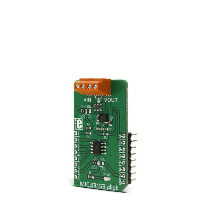
The MIC33153 click has two robust screw terminals for connecting the input and output voltage rails. Instead from the input terminal, the click can use the voltage input from the development system itself if VIN SEL SMD jumper is switched to the VCC position (default jumper position). MIC33153 click can work with both 3.3V and 5V rated MCUs. To select the desired operational voltage, the VCC SEL SMD jumper should be switched to the correct position, indicated by the label – 3.3V or 5V. It should be noted that the selected voltage will be used as the internal voltage supply for the buck converter input, if selected so by the VIN SEL. Also, 3.3V is required regardles of the position of the VCC SEL jumper, since the MCP4921 DAC is powered up from 3.3V rail, directly.
Specifications
| Type | Buck |
| Applications | Power supply for the various portable GPS devices, mobile handsets, portable media and mp3 players, wireless LAN cards and similar applications that demand very clean power supply and high step down DC-DC conversion efficiency factor. |
| On-board modules | MIC33153 a 4MHz DC-DC buck regulator with integrated inductor and Hyperlight Load™ technology, and MCP4921, a 12bit DAC converter with the SPI interface, both from Microchip. |
| Key Features | High efficiency and low output voltage ripple throughout the whole load range, soft start feature, thermal shutdown and current limit protection, up to 1.2A of current, HyperLight Load™ technology, adjustable output voltage and power good indication |
| Interface | GPIO,Analog,SPI |
| Input Voltage | 5V,3.3V |
| Click board size | M (42.9 x 25.4 mm) |
Downloads
Fast Shipping and Professional Packing
Through our long-term relationship in a long-standing partnership with UPS, FedEx, DHL and many other top global carriers we can provide a variety of shipping options. Our warehouse employees will pack every item to our exacting specifications. The goods you send us are checked thoroughly and secured properly prior to shipping. Everyday we deliver thousands of packages to customers across many countries. The fact that we're committed to becoming the biggest online retailer in the world is clear. Both Europe as well as the USA have warehouses and distribution centres.
Orders that contain more than one item are assigned processing times in accordance with the item.
We will inspect each and every one of the items ordered before shipping. Today, most orders will be shipped within 48 hours. The delivery time should be between 3-7 days.
Returns
The stock market is always changing. It's not entirely managed by us, since we have multiple organizations, such as the factory and our storage. Stock levels can fluctuate at any given time. Please understand it may happen that your order will be out of stock after the order is placed.
The policy is for 30 days. If you have passed 30 days in the past since you purchased, unfortunately we can't offer you a refund or exchange.
To be eligible for a refund, your item must be in good condition and in the same state that you received it. The item must be in the original packaging.
Related products
Power Module
Power Module
Battery Holder
Power Adaptor
Battery Holder
Power Module
Battery Holder
Battery Holder
Power Adaptor
Battery Holder
Serial Comms
Power Adaptor
Power Module
Power Module
Battery Holder
Power Adaptor
Power Module
Power Module
Solar Power Manager Embedded 10000mAh Li-Po Battery, Supports 6V~24V Solar Panels Waveshare
Power Module
MIC23099 click – MikroElektronika Single AA/AAA Battery Cell Regulator MikroElektronika
